Surface-Enhanced Raman Spectroscopy of 2D Organic Semiconductor Crystals
Dmitry R. Maslennikov, Andrey Yu. Sosorev, Roman S. Fedorenko, Yuriy N. Luponosov, Sergey A. Ponomarenko, and Vladimir V. Bruevich.
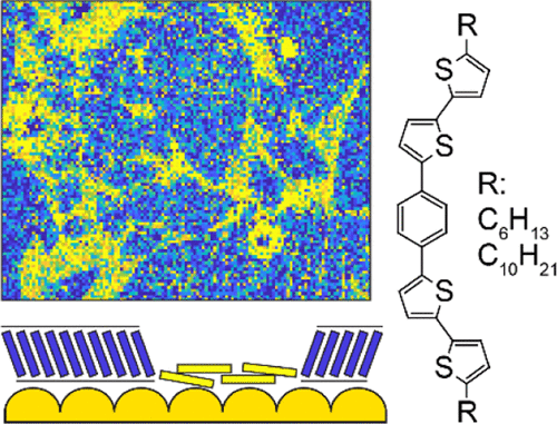
Recently developed ultrathin two-dimensional (2D) organic semiconductor crystals are a promising platform for advanced organic electronic devices. Remarkable quality of such crystals results in charge-carrier mobilities comparable to those of bulk crystals, but their structure and orientation are hard to study because of their extremely small thickness. Here, we applied surface-enhanced Raman spectroscopy (SERS) to investigate the structure of the thinnest 2D single crystals—monolayers, which are based on thiophene-phenylene co-oligomers: 1,4-bis(5′-decyl-2,2′-bithiene-5-yl)benzene and 1,4-bis(5′-hexyl-2,2′-bithiene-5-yl)benzene. Their Raman spectra were calculated as a function of the molecule orientation and SERS microscopy maps were acquired. High sensitivity of SERS allowed us to study monolayer single-crystal domains with the optical spatial resolution. Raman anisotropy was used to probe the orientations of single-crystal domains and the molecule orientation within them. Notably, the SERS microscopy detected the presence of a submonolayer—amorphous material between the crystalline domains, which is practically inaccessible to optical or conventional atomic force microscopies (AFMs). The submonolayer was also studied by lateral-force AFM, which showed notably higher friction and adhesion. We found that the measured Raman anisotropy significantly reduced by the metal-covered substrate still allowing us to distinguish orientations of molecules in the 2D crystals and in the submonolayer. Anisotropy-sensitive SERS was shown to be promising for studying 2D organic semiconductor crystals.